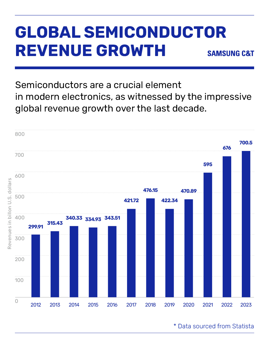
In almost all electronic devices we use these days, from smartphones that help us in daily life to spacecraft that are considered the pinnacle of science, semiconductors are required to function. The growing importance of semiconductors is shown by the solid and impressive revenue growth from sales in the last decade.
Producing semiconductors, which have become smaller and more advanced over time, takes highly specialized manufacturing facilities. Samsung C&T’s Engineering & Construction Group is accelerating its business of constructing such facilities inside and outside Korea.
What is a fab?
A “fab” is short for fabrication facility or fabrication plant; in other words, a specially designed factory that manufactures semiconductors. As a powerhouse in information technology and electronics, Korea needs more and more fabs to produce its advanced, cutting-edge technology.
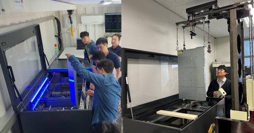
The heart of every fab is its so-called “clean room.” As the name suggests, it is a strictly controlled environment with the highest standards of cleanliness. The temperature, humidity, and vibration of a clean room must be minutely regulated to shield the semiconductors from external factors because even the smallest particles or process interruptions can cause product defects.
Apart from the clean room, a fab supplies the high-purity gas, water, and electricity required for production. Also, each fab is equipped with expensive and sensitive machines that make up the production process.
Since the internal mechanisms are so specialized, the building of a fab itself is a complex process beginning with planning, programming, and design, continuing through production, inspection, and installing equipment, and ending with start-up. Afterwards, total productive maintenance keeps the fab operational and allows for improvements.
Fabs around the world
Samsung C&T’s Engineering & Construction Group is recognized for its global technology and capabilities in carrying out multiple semiconductor fab construction projects at home and abroad. Recently, Samsung C&T’s Engineering & Construction Group obtained a contract to construct a semiconductor consignment production plant in Taylor, Texas, and in September foundation work began at the P4 fab complex for Samsung Electronics in Pyeongtaek.
In addition, Samsung C&T successfully carried out the Hwaseong line 17 fab finishing project by Samsung Electronics and Amkor Korea’s K5 project to build a Global R&D Center and semiconductor factory.
Samsung C&T E&C Group provides services throughout the project’s entire life cycle, including participation from the planning and construction stages and consulting in the operation stage, based on its accumulated cutting-edge technology and experience in private-sector construction.
In addition to its work for the semiconductor industry, Samsung C&T E&C Group is taking advantage of its professional capabilities and experience by carrying out high-tech production complex projects for the solar panel and biopharmaceutical industries.
Based on its expertise, the group plans to carry out high-tech production complex projects for solar panels and biopharmaceuticals in addition to the semiconductor business.